
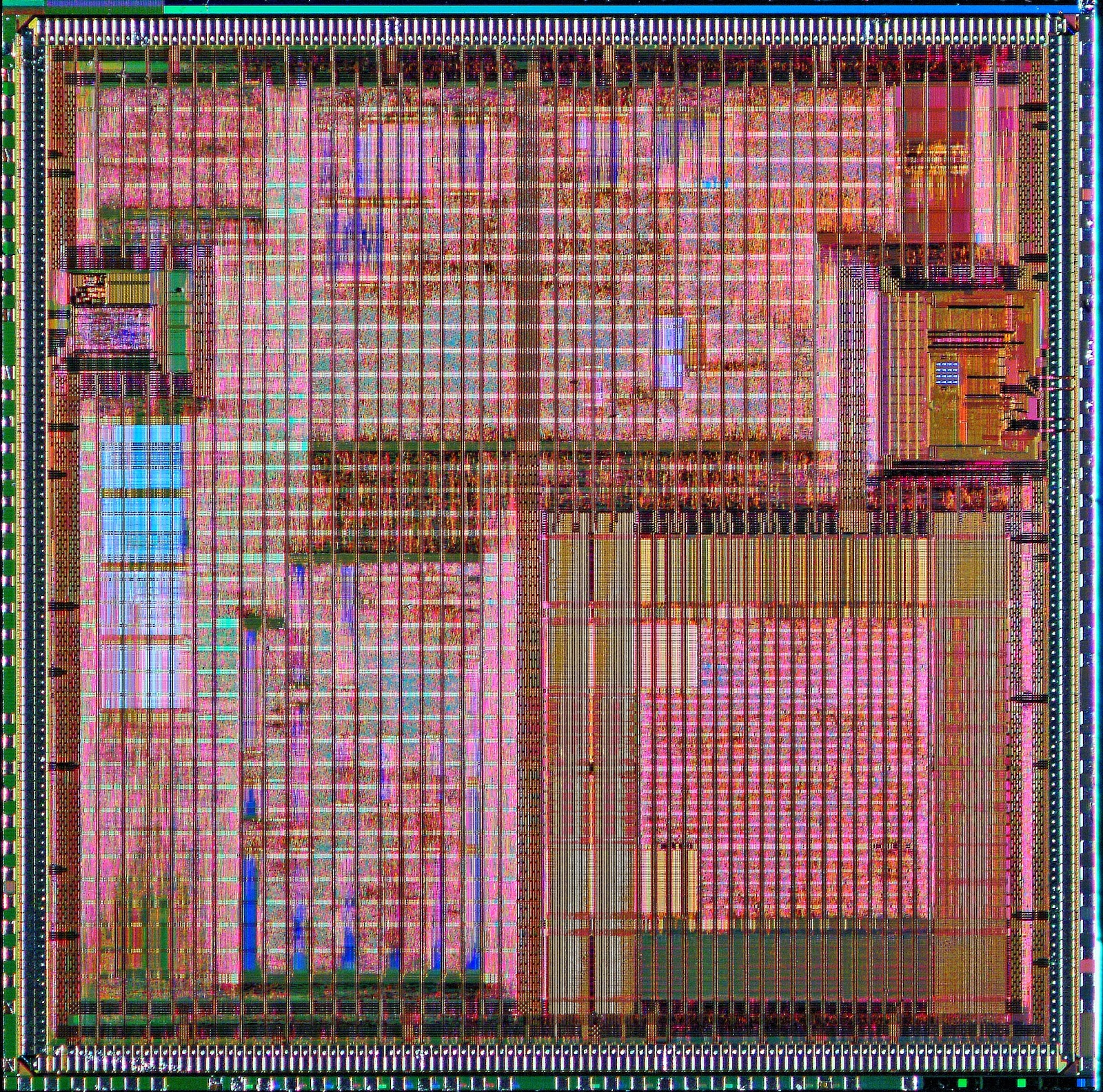
Are you looking for a good test of your patience, you lighting skills, your manual dexterity and you photographic technique? You might want to try your hand at the devilishly hard process of photographing the innards of microprocessor and micro controller chips. If they are lit correctly you can get some interesting patterns and colors. But you'll need to get a lot more magnification than you'll get out of that 50mm macro lens attached directly to your DSLR camera....
At one point back in 2004 we were photographing eight or ten sets of chip dies a month for the folks at Motorola. They had two big fabs in Austin and it was a time in which the hardware side of the tech business was booming.
I'd get a phone call from someone in marketing and I'd head over an pick up a heavy duty plastic container with tiny, tiny little squares of silicon with even tinier photo etched circuits on them. The clients needed clean, colorful photographs that they could blow up big and use in printed brochures and magazines, and it was always a bonus if we could make them high enough resolution to print onto 4x4 foot wall posters. It was always a big "ask" with a miniature deadline.
I'd haul the little squares back to the studio and start assembling the macro rig. A very rigid copy stand with a camera holder on rails so that one had two levels of control of lowering the camera toward the subject. But between the camera and the subject was a bellow that sometimes extended nearly twelve inches along with a specialized macro lens that was optimized for magnifications between 3x and 8x life-size.
There were three hellacious speed bumps we had to deal with on almost every job. One was getting hard light onto the subject from just the right angle to create a visual representation of the information on the surface (actually, several layers of surface). The second challenge was to keep the small (and very light) wafer in place and plano-parallel to the lens stage and the "film" stage of the camera. We cheated and used a little bit of spray mount painted on a holder surface with a toothpick.
We had to secure the chip so we could "puff" it with compressed air just before shooting so we could make sure that we didn't get giant piles of dust in the photo. Retouching was out of the question. Too much fine detail.
If we used compressed air on an un-anchored die it would go flying off into the infinite clutter of the studio.
The colors and the details were dependent not just on the angle of the lights but also on the aperture of the lens. Diffraction and fall off limited anything smaller than f5.6 and sometimes our best shots were at the widest aperture of f2.8. Changing apertures meant that the focus changed and that meant a whole new round of re-focusing.
The final challenge was vibration and movement from the camera shutter. When the chip sizes went under a certain size we started to depend on opening the shutter with a black card under the lens, moving the black card and counting out "one elephant, two elephant...." and then replacing the card. No vibration --- as long as we didn't touch anything.
If I was lucky I could get a good shot in a couple of hours. All of these images are from the same chip product. They are a result of changing the light angles, changing the elevation of the lights and changing the size of the light surface. The experiments (and re-focusing would go on until I got a handful of successful images and then it would be another hour in post processing.
We started doing this kind of work back in the film days. A really good chip die shot could take a day to get just right because every bout of trial and error required Polaroid testing and then more testing.
Our first foray into chip shooting was for the Apple/IBM/Motorola consortium that came together to create the RISC based PowerPC chip family. The last Motorola conference I attended was still using an 8x8 foot blow up of the original PowerPC chip I had taken (on large format film) nearly a decade earlier...
A bigger challenge was getting a good die shot of the first IBM multi-core processor. Security in the pre-announcement stage was so high I had to take all my stuff and head over to their offices where I juggled a full sized 12 inch wafer filled with the little squares while a marketing person hovered close by. We processed the images on site and then they "helped" me to erase my CF card just in case....
Makes for a pretty iron clad NDA.


4 comments:
Great colours! I remember doing something similar in the early 90's and nearly setting fire to some hassleblad bellows with very bright tungstens :(
Almost looks like you can see the "Ghost" in the machine. Nice work!
Rob Morrris
Cool stuff. Hard to imagine doing stuff like this before digital. Polaroid was a life saver.
Masterful.
Post a Comment